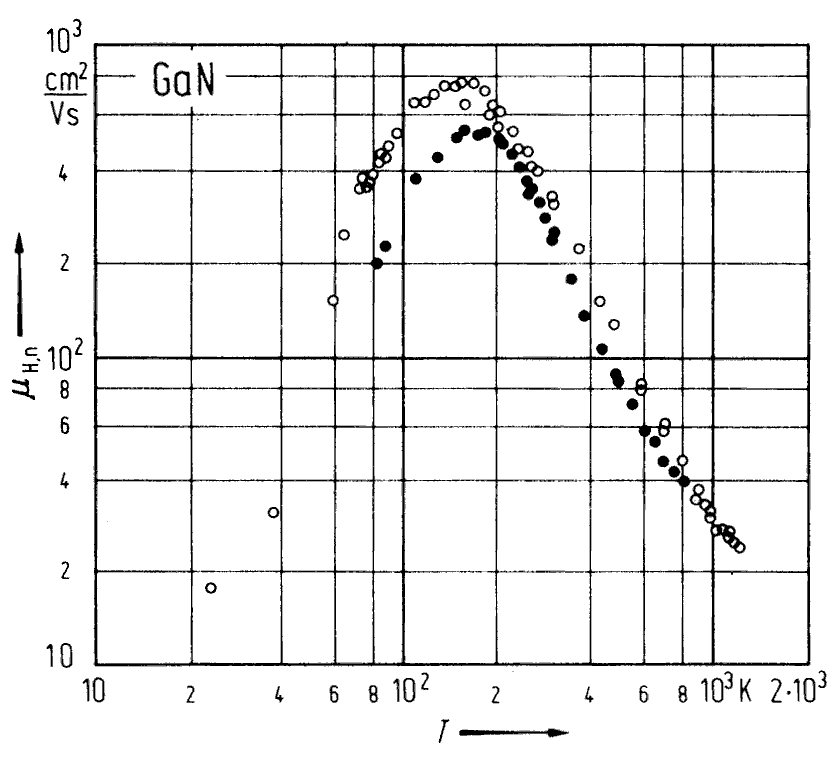
Ilegems & Montgomery (1973).
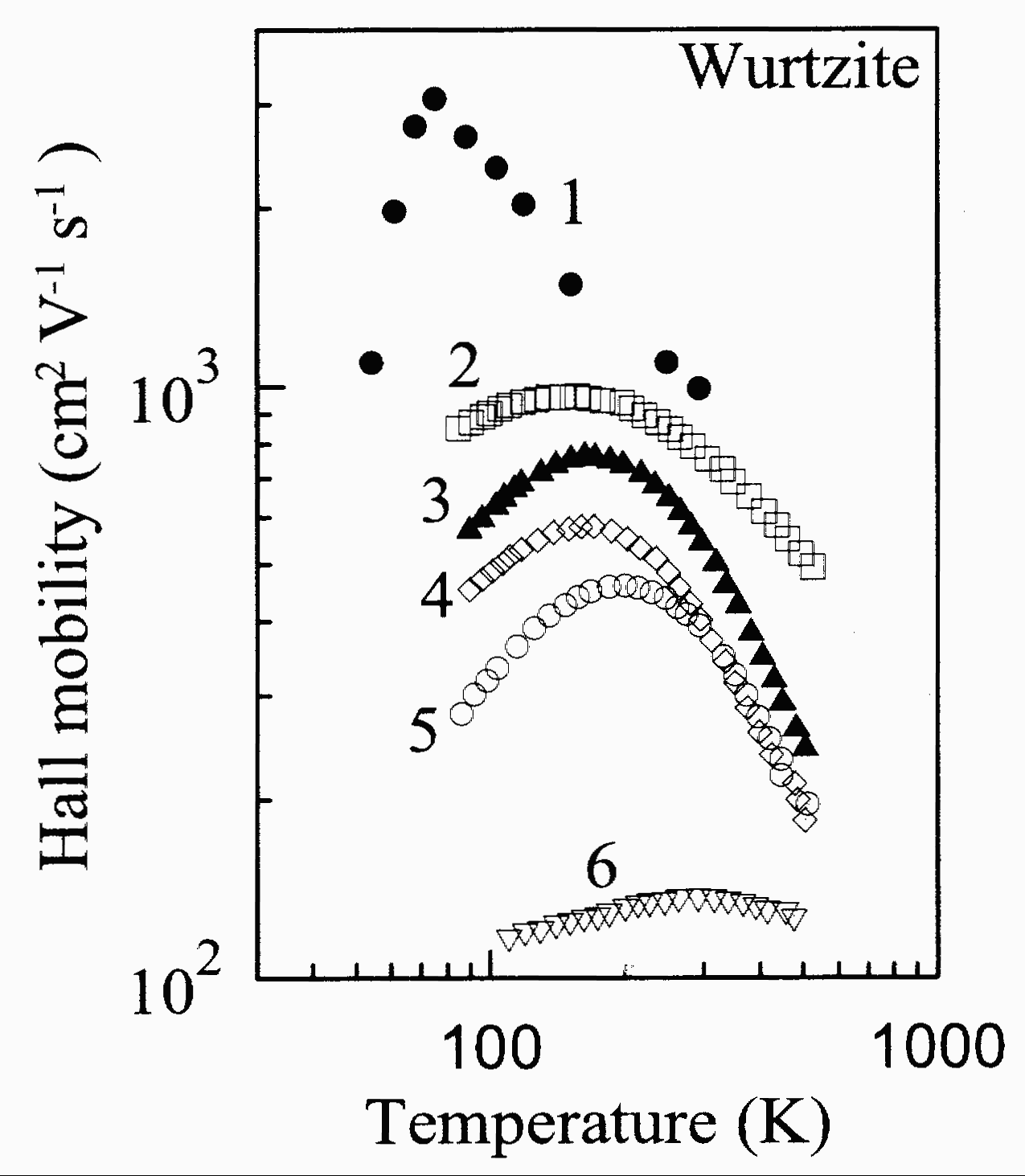
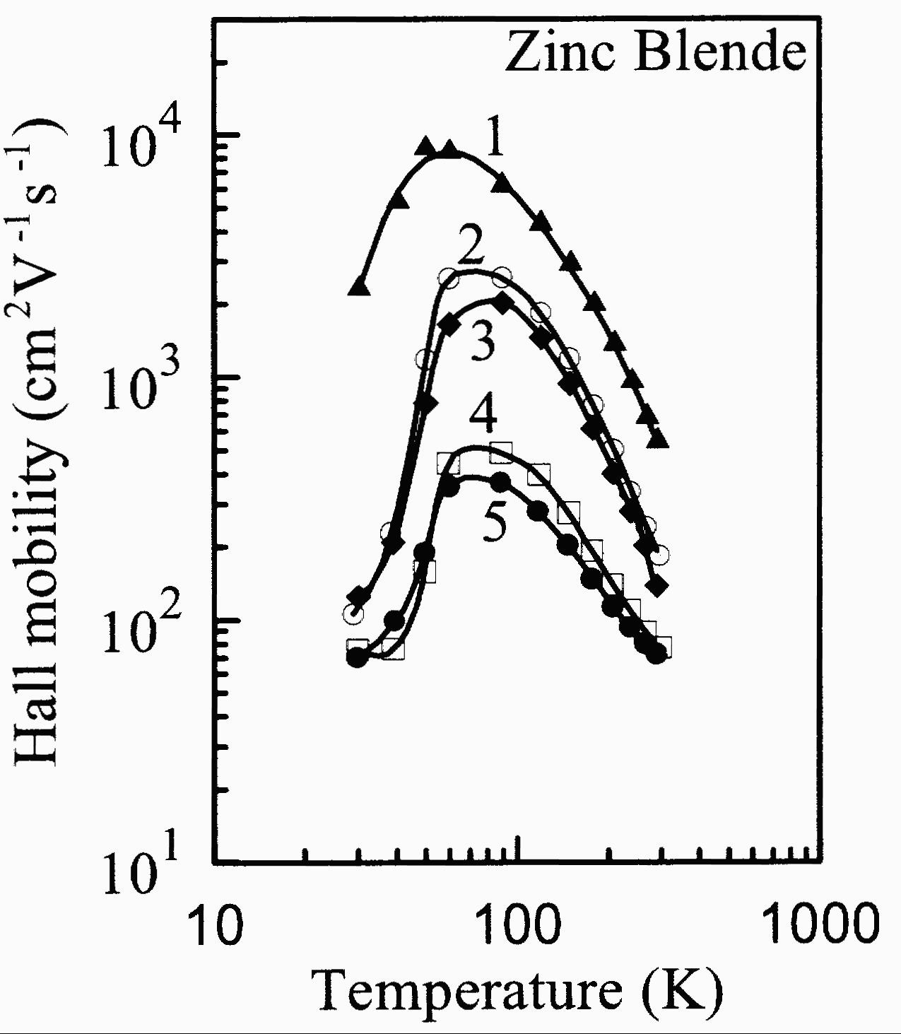
1 - unintentionally doped [Nakamuraetal.(1992)];
2 - Nd = 3.1x 1017 cm-3, θ < 0.03 [Gotz et al. (1996)];
3 - Nd = 1.1 x 1017cm-3, θ ~= 0.3 [Gotz et al. (1996)];
4 - Nd = 2.3 x 1017 cm-3, θ < 0.04 [Gotz et al. (1996)];
5 - Nd = 7.4 x 1017 cm-3, θ < 0.01 [Gotz et al. (1996)];
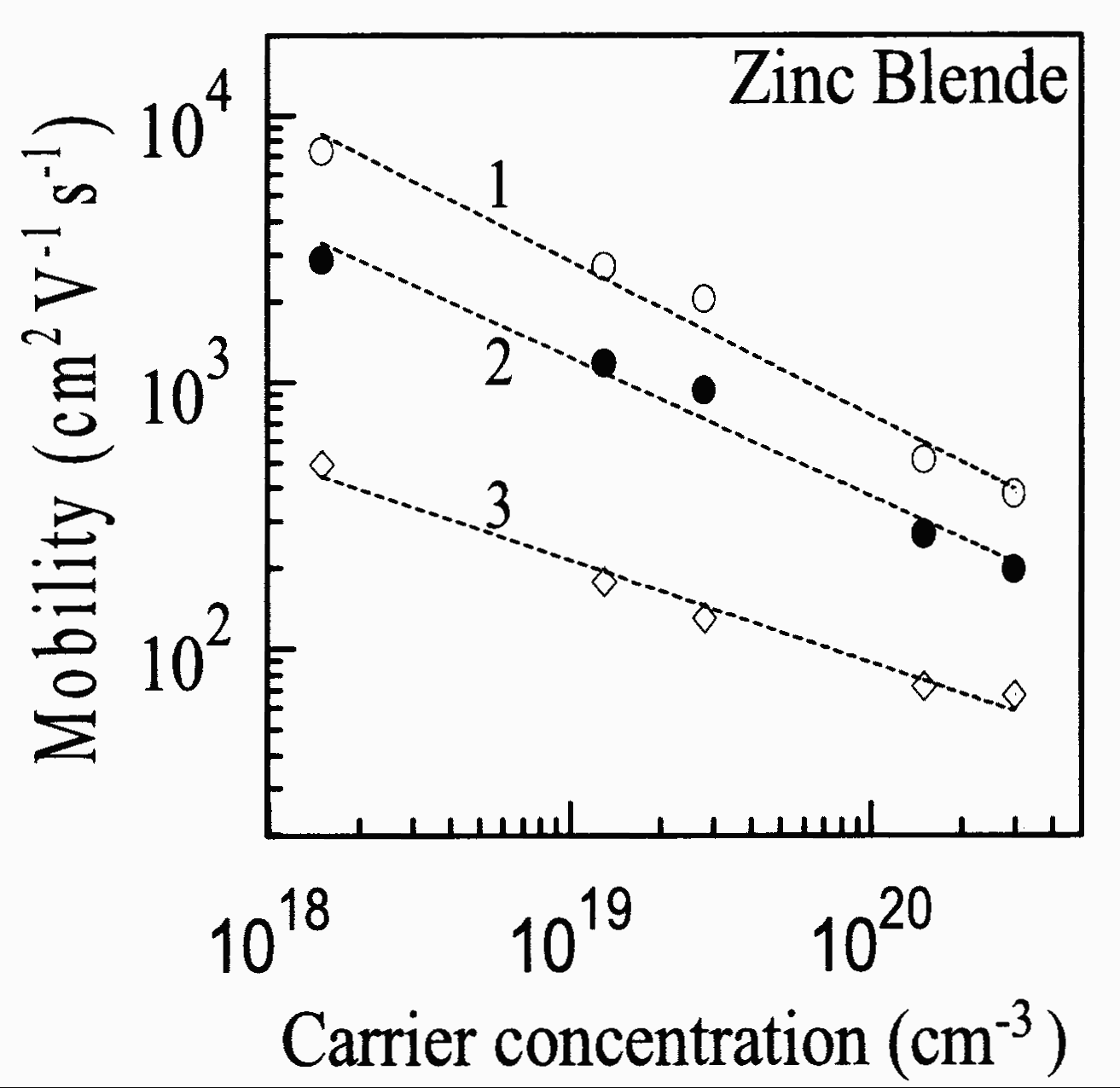
6 - The concentration of introduced Si Ndo = 2 x 1019cm-3 [Gotz et al. (1996)].
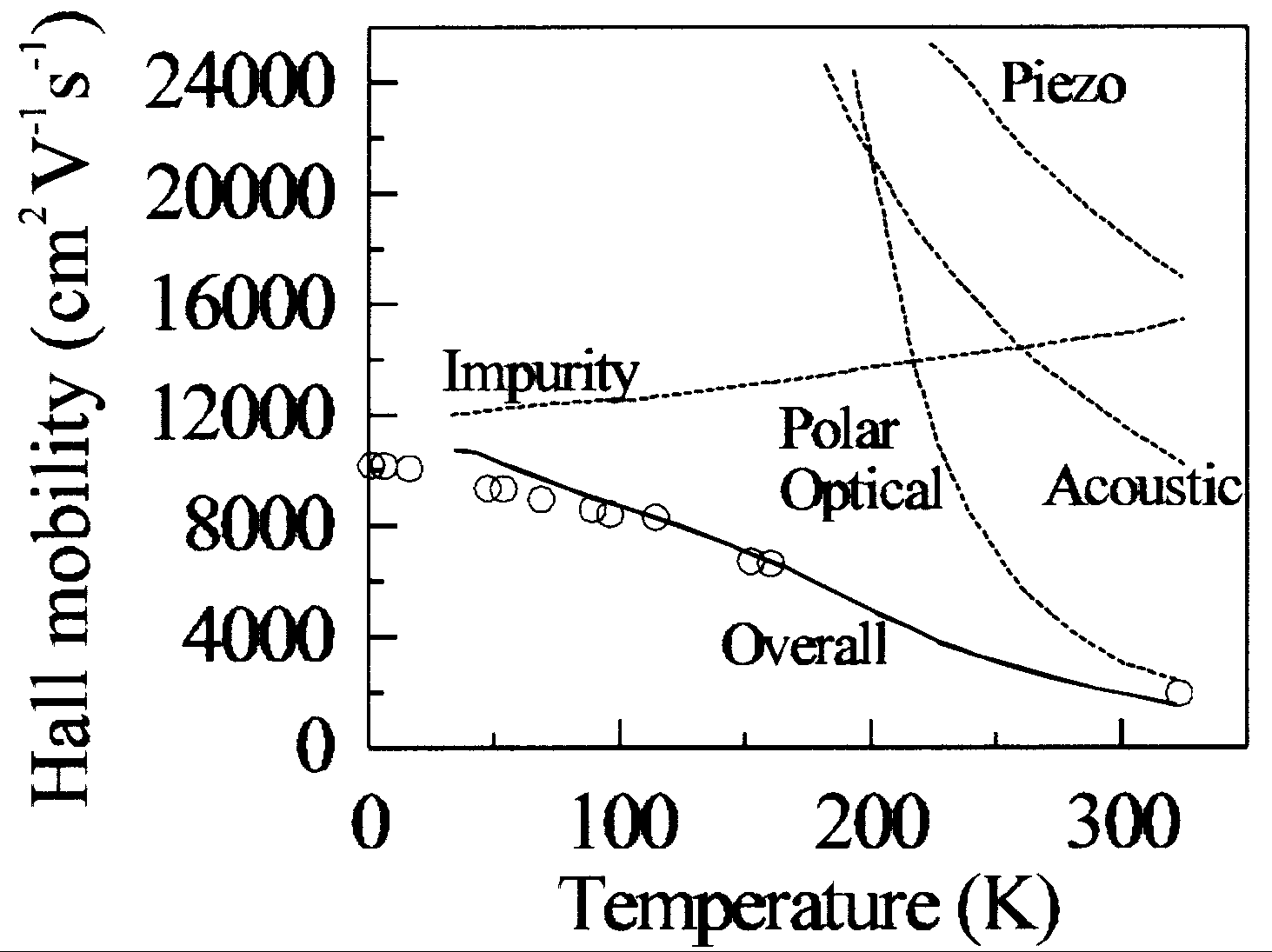
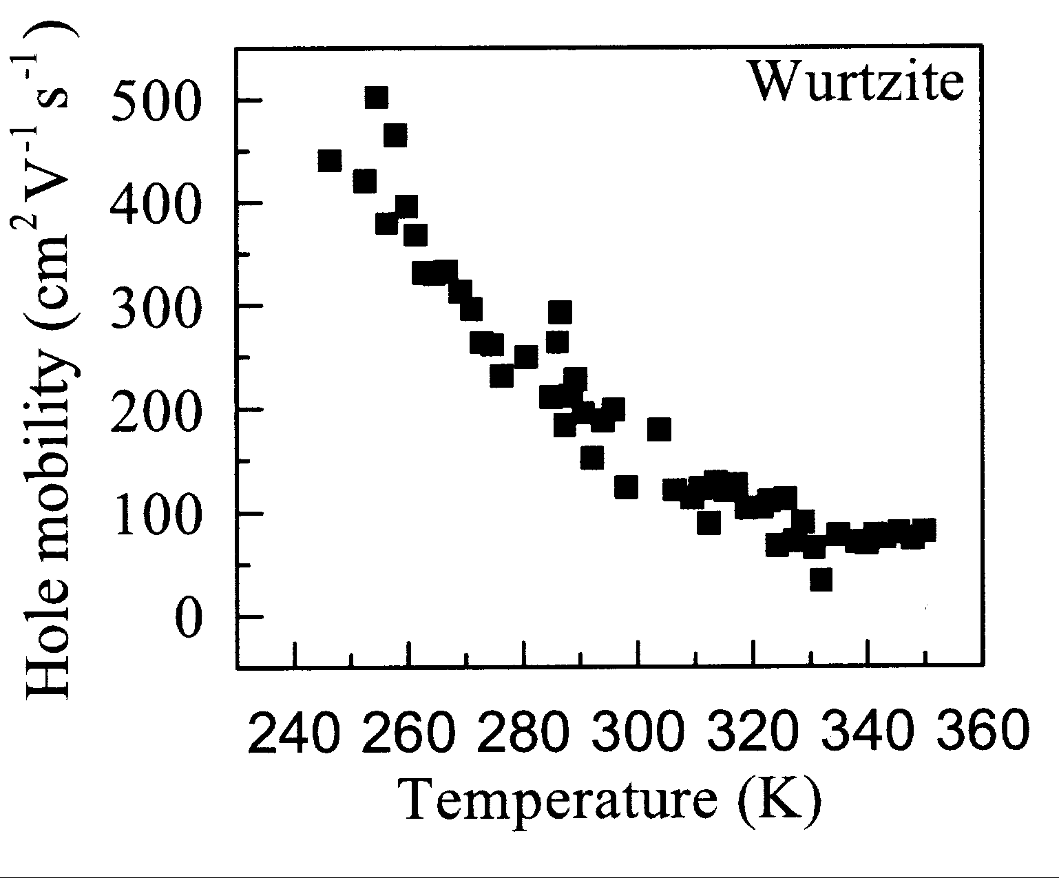
The calculations of electron mobility vs. the temperature for different doping levels and compensation ratios see in Chin et al. (1994).
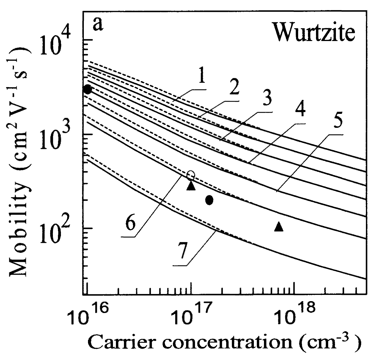
1 - θ = 0; 2 - θ = 0.15;
3 - θ = 0.30; 4 - θ = 0.45;
5 - θ = 0.60; 6 - θ = 0.75; 7 - θ = 0.90.
T = 77 K. Experimental data are taken from four different papers
Chin et al. (1994).
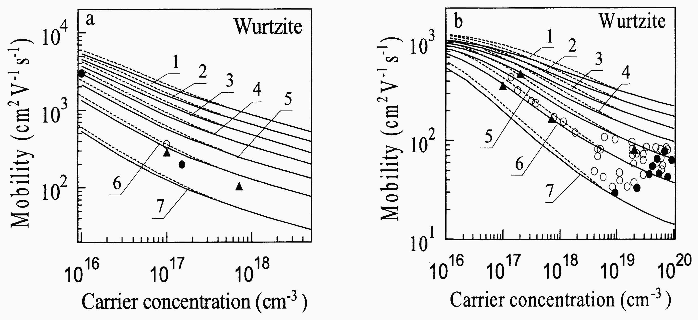
1 - θ = 0; 2 - θ = 0.15;
3 - θ = 0.30; 4 - θ = 0.45;
5 - θ = 0.60; 6 - θ = 0.75; 7 - θ = 0.90.
T = 300K. Experimental data are taken from four different papers
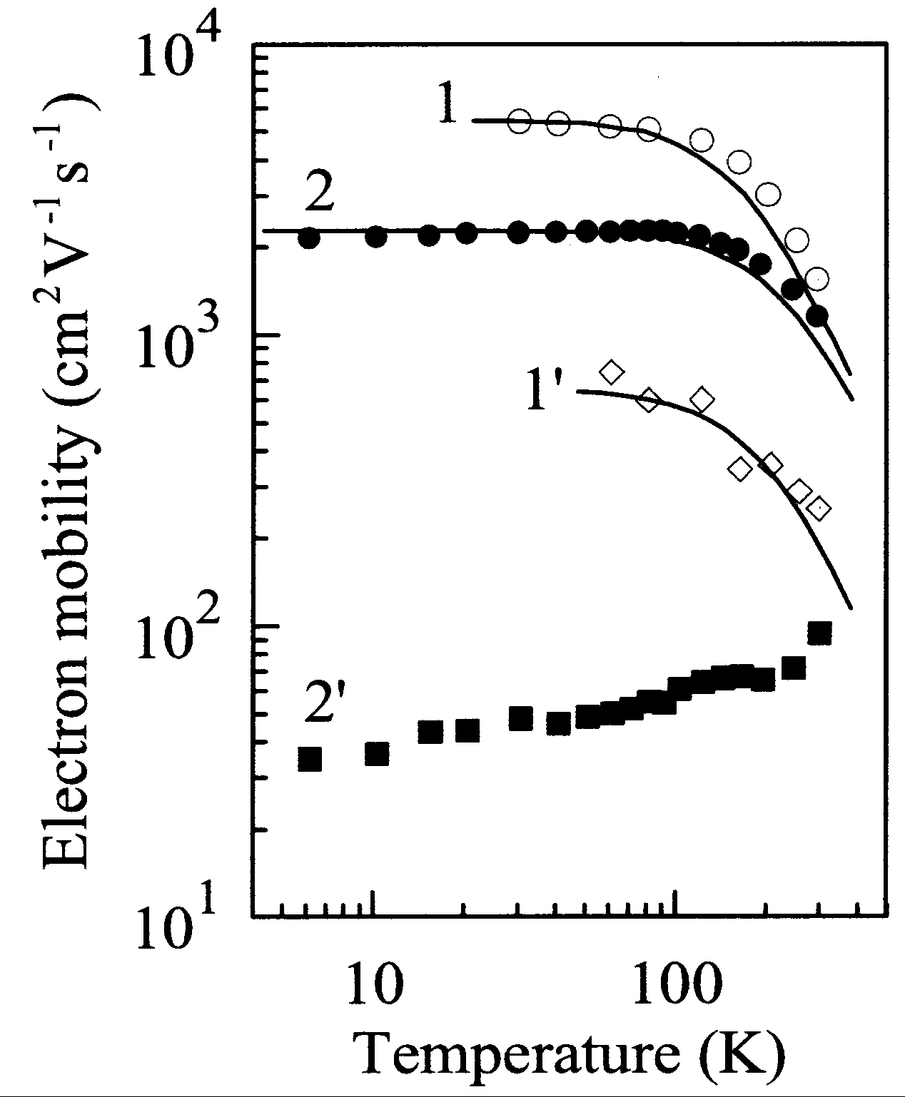
Chin et al. (1994).
Rubin et al. (1994).
Gaskill et al. (1995).