|
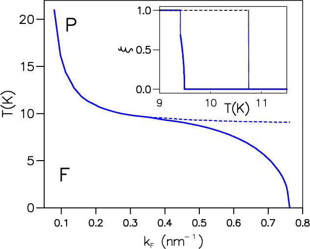
Phase diagram of a DMS quantum well, using the parameters described in the text. Full and broken lines represent
first- and second-order phase transitions, respectively, between ferromagnetic (F) and paramagnetic (P) phases. In the inset we
show the carrier spin polarization for two different densities. The broken line corresponds to kF = 0.2 nm-1, in this case there is
a first-order transition between the x = 1 ferromagnetic phase and the paramagnetic phase. The continuous line corresponds to
kF = 0.39 nm-1. Upon lowering the temperature we obtain a continuous transition between the P and the F phases followed by
an abrupt transition between two F phases with different values of x . As commented in the text, this last
transition is probably spurious. |