Overview of research activities
Task 1: Theoretical studies of the mechanisms of the AAS oscillations revealed by the spin interference due to the Rashba SOI
in the gate-controlled AB rings are underway to define the relative contribution from the change of concentration and the
spontaneous spin polarization of the carriers.
Milestone a: The AAS oscillations in a double-slit one-dimensional ring. The spin-interference that is caused by the Rashba spin-orbit interaction (SOI) in a gate-controlled two-terminal Aharonov-Bohm ring has been studied by the analysis of the Aharonov-Casher (AC) and Aharonov-Bohm (AB) conductance oscillations that appear to be revealed respectively as a function of both the gate voltage and magnetic field [1]. The scattering matrix approach was used to exhibit the effect of the quantum scatterers that represent the quantum point contacts (QPCs) connected to two one-dimensional leads on the phase of the transmission and reflection amplitudes [2]. The variations of the transmission and reflection amplitudes that are caused by the quantum scatterers for the particles moving inside and outside the Aharonov-Bohm ring have been shown to define a parity of the h/e and h/2e conductance oscillations thereby verifying the relative contribution from the Aronov-Altshuler-Spivak (AAS) conductance oscillations [3]. The results of numerical calculations demonstrate the progressive enhancement of the quasi-periodicity of both the AC and AB oscillations, which plot specifically as a gradual transformation of the 2e2/h plateaus in the 2e2/h pronounced peaks as a function of the Rashba SOI parameter and the value of the external magnetic field [2]. The h/2e harmonic is of importance to dominate over the h/e harmonic already in a slight effect of the quantum scatterers on the conductance of the AB rings. Thus, the particles moving in the clockwise and anticlockwise direction are scattered by the QPCs that seems to enhance the variations of the amplitudes and the phase of the AC and AB oscillations which have been observed in the gate-controlled AB rings [4-10] and to influence on the amplitudes of the AB oscillations found by studying the double-slit AB rings with the quantum dot inserted in one of its arms [11]. The experimental investigations of the spin-interference revealed by the Rashba SOI in the top gate-controlled three-terminal AB ring that contains the drain and source QPCs and the extra-QPC inserted in one of its arms by the split-gate method have verified for the first time the theoretical dependences obtained within frameworks of the models based on scattering on these QPCs [12-16]. The AC and AAS conductance oscillations found in the three-terminal one-dimensional rings embedded in the plane of the p-type silicon quantum well (Si-QW) prepared on the n-type Si(100) surface have been shown to result from the scattering of holes on the QPCs inserted. The relative contribution from the AC and AAS conductance oscillations to the spin-dependent transport in the absence of changes in the sheet density and mobility of holes has been analysed by varying the top gate voltage that controls the amplitude of the 0.7∙(2e2/h) feature in the quantum conductance staircase due to the extra-QPC that has been fixed by the split-gate voltage [15, 16]. Indeed, the only short range of the top-gate voltage where the sheet density and the mobility of 2D holes are low and stable can be used to divorce the AC conductance oscillations caused by the Rashba SOI from the other effects such as the Fermi resonances. The value of the effective mass of the heavy holes, meff, in the p-type Si-QW estimated from the relationships introduced by Winkler et al [17] for the period of the AC conductance oscillations as 6.7 10-4 m0 appeared to be in a good agreement with the data of the CR measurements and the temperature dependences of the SdH oscillations. Owing to such small value of meff that is due to the properties of the δ-barriers confining the Si-QW and the presence of the ultra-shallow p+-n bias junction, these measurements of the spin interference have been realised at T=77 K [12-16]. Finally, the transmission phase shift has been also revealed by the AC conductance oscillations measured by varying the top gate voltage applied to the two-terminal device with the only drain and source constrictions [7, 8]. However, the variations in the sheet density of carriers that accompany the application of the top gate voltage are also able to give rise to the conductance oscillations which result from the variations in the value of the Fermi wave vector. Therefore the three-terminal device with the quantum dot (QD) [11] or the quantum point contact (QPC) [12-16] inserted in one of the ring's arms using the split-gate technique could be more appropriate to divide the relative contribution of the AC effect in the conductance oscillations.
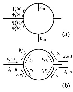
FIG.1. Schematic view of a spin-interference device [15, 24] that is based on the AB ring connected with two one-dimensional leads by QPCs and covered by the gate electrode that controls the Rashba SOI. (a) The spin directions of the clockwise and anticlockwise travelling electronic waves. (b) The amplitudes of travelling electronic waves 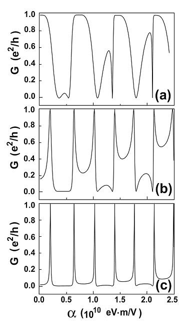
FIG.2. The AC oscillations calculated at different values of the transmission amplitude from a lead to the AB ring (from the AB ring to a lead). (a) ε=0.707; (b) ε=0.507; (c) ε=0.307. 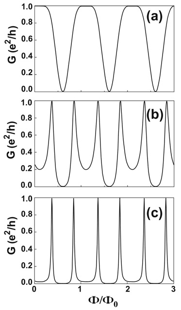
FIG.3. The AB oscillations calculated at different values of the transmission amplitude from a lead to the AB ring (from the AB ring to a lead). (a) ε=0.707; (b) ε=0.507; (c) ε=0.307. 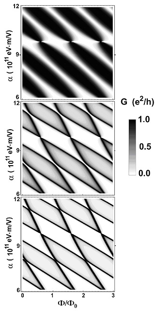
FIG.4. Grayscale plot of vs and (a) ε=0.707; (b) ε=0.507; (c) ε=0.307 |