Leading by
The team has a well recognized experience in the acoustical studies of
the high-frequency (HF) conductivity in the nanostructures.
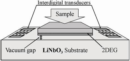
Schematic of the acoustoelectric device: The
electric field of a surface acoustic wave propagating on the surface of
a piezoelectric substrate acts on a low dimensional electron
system “embedded”
into the sample close to its surface. This “hybrid” geometry
allows applying a sliding electrostatic potential to the electron/hole
system in nonpiezoelectric materials.
In the course of the studies on the GaAs/AlGaAs heterostructures in the
quantum Hall (QH) regime it has been shown that in magnetic fields H
corresponding to the Hall's plateau, when the electrons are localized,
the acoustoelectric effects are governed by the hf hopping
conductivity. The latter is not equivalent to the dc conductivity and
is a complex quantity. Both real and imaginary parts are obtained by
simultaneous measurements of the attenuation and velocity change of the
surface acoustic wave (SAW). This is a pioneering result that allows us
to successfully promote a new scientific approach to the study of the
localized states of the two-dimensional electrons in the QH-regime [1].
It should be noticed that dc-studies of these objects could not be
performed at the Hall's plateau centre, the dc conductivity at the
corresponding H=0.
HF-conductivity in the modulation-Si-doped GaAs/AlGaAs heterostructures
has been studied by the acoustoelectric method also. It has been shown
that in the QH regime the hf hopping conductivity of the 2DEG layer is
effectively shunted by that of the AlGaAs doping region. A method to
separate these two contributions to the hf-conductivity in the QH
regime has been put forward, and the localization length in the
corresponding H evaluated.
It has been observed that both the hf hopping conductivity and the
carrier density in these samples depend on the rate of the sample
cooling, illumination, and stress. An energy threshold there exists at which the frozen hf hopping
photoconductivity takes place. This result is attributed to the
so-called DX-centers [2].
For the first time, this contactless acoustic method was applied for
the monitoring of the Si/SiGe heterostructures in the IQHE regime. The
absorption and velocity shift of the SAW have been measured in the IQHE
regime.
Since neither Ge, nor Si are piezoelectrics, the only way to measure
the acoustoelectric effects in the systems is a hybrid method when a
SAW propagates along a surface of a piezoelectric, while the sample is
placed on its surface. In this case only the electric field of the SAW
penetrates into the Si/SiGe sample.
Dense arrays of Ge quantum dots in Si host were studied using the
acoustical method. The measured temperature dependencies of the DC
conductance of the same samples evidence the variable range hopping
(VRH) in the Coulomb gap regime.
Quantum oscillations of SAW attenuation and velocity in the GaAs/AlGaAs
heterostructures in the case of spin-splitted Landau bands have been
observed and investigated. It allowed one to obtain the electronic
g-factor value for the 2DEG, which appeared to be near an order higher
than the g-factor for the bulk GaAs [3, 4].
All the results cited above confirm the ability of the team to perform
acoustoelectric measurements in the nanosystems of different type.
Experimental Technique in Use: He3 low temperature setup T=0.3-4.2K,
magnetic fields up to 7T. Operating frequencies f=30-300MHz.
Top panel: magnetic field dependences of the SAW attenuation, Г, and of the
relative velocity change, DV/V for
frequency f=30 MHz.
Bottom panel: components of the complex high-frequency conductivity
s1 and s2 of ac
conductivity versus magnetic field H at T=1.5 K. Sample is the GaAs/AlGa heterostructure.
The last update was made on November 25, 2004
Web-Master