
Forum
"Nitrides" on NSM-archive
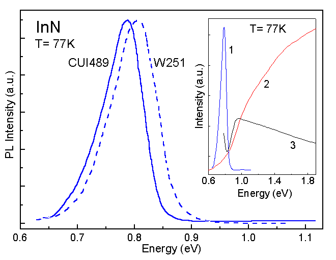 |
InN, Wurtzite (hexagonal). Photoluminescence spectra for samples
with different electron concentrations: n ~ 9x1018 cm-3 (MOMBE grown sample CUI489); n ~1.2x1019 cm-3 (PAMBE grown sample W251). The inset shows the spectra for the sample with electron concentrations of n ~ 9x1018 cm-3 (CUI489): 1 - photoluminescence; 2 - optical absorption; 3 - photoluminescence excitation. Davydov et al. Phys. Stat. Solidi (b) 229 (2002a), R1 Contact authors: Valery Yu. Davydov Remark. It was the first observation of edge photoluminescence in near-infrared region in single-crystalline InN . |
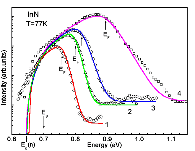 |
InN, Wurtzite (hexagonal). Photoluminescence spectra of
InN layers with different carrier concentrations. 1 - n = 6x1018 cm-3 (MOCVD grown sample); 2 - n = 9x1018 cm-3 (MOMBE grown sample); 3 - n = 1.1x1019 cm-3 (MOMBE grown sample); 4 - n = 4.2x1019 cm-3 (PAMBE grown sample). Solid lines show the theoretical fitting cures based on a model of interband recombination in degenerated semiconductors. As a result, the true value of InN band gap Eg~0.7 eV was established. Davydov et al. Phys. Stat. Solidi (b) 230 (2002b), R4 Contact authors: Valery Yu. Davydov |
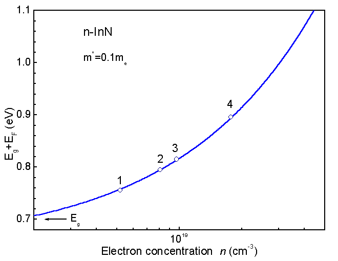 |
InN, Wurtzite (hexagonal). Calculated shift of optical absorption edge
due to the Burstein-Moss effect in n-type InN (solid line) vs. electron
concentration. The parabolic conduction band with an effective electron mass of m*=0.1 mo is assumed. Open circles present the values ( Eg + EF) estimated from the fitting of photoluminescence spectra. Davydov et al. Phys. Stat. Solidi (b) 230 (2002b), R4 |
|
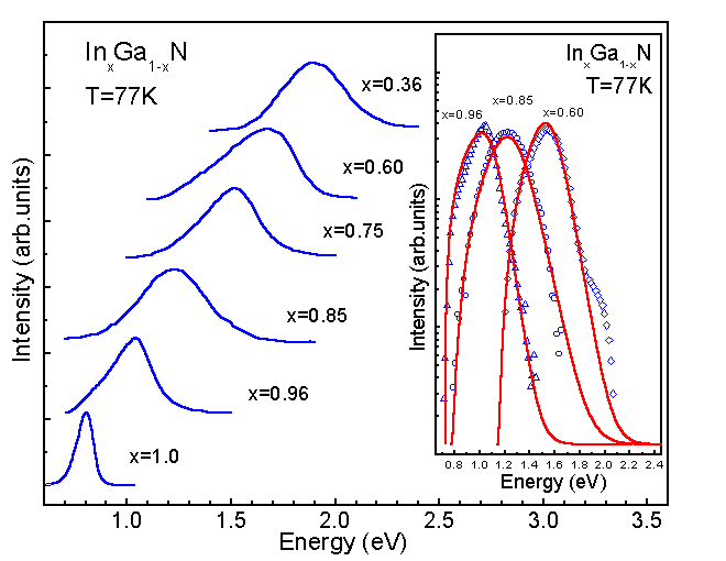
In-rich InxGa1-xN alloys. Photoluminescence
spectra of layers with different compositions at T=77 K. The inset shows the semilog photoluminescence spectra of most perfect alloys and the fitting cures of the spectra based on a model interband recombination in degenerated semiconductors . Davydov et al. Phys. Stat. Solidi (b) 230 (2002b), R4 Remark. It was the first observation of edge photoluminescence in single-crystalline in-rich InxGa1-xN alloys (0.36<x<1). |
|
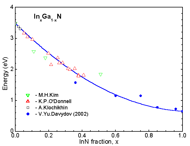
InxGa1-xN alloys. The Eg valus
estimated for In-rich alloys (full blue circles, this work), and positions
of photoluminescence band maxima in Ga-rich alloys (open symbols) as a function
of InxGa1-xN composition. Composition dependence of the band gap (solid line) is fitted by equation Eg(x)=3.493 - 2.843x - bx(1-x) with a bowing parameter b=2.5 eV. Refs.: M. H. Kim, J. K. Cho et al., Phys. Stat. Sol.(a) 176, 269 (1999); K. P. O'Donnell et al., J. Phys. Condens. Matt. 13, 6977 (2001) ; A. Klochikhin, A. Reznitsky et al., Nanostructures: Physics and Technology, Ioffe Institute, St. Petersburg 2001, p.554. Davydov et al. Phys. Stat. Solidi (b) 230 (2002b), R4 |
 |
InN, Wurtzite (hexagonal). (a) Optical absorption (300 K),
photoluminescence (300 K), and PR (77 K) spectra. This sample is undoped
with room-temperature electron concentration of n=5.48x1018 cm-3.
The spike on the PR spectrum at 0.97 eV is an artifact due to the light
source used in the PR measurement. (b) Room-temperature mobility, photoluminescence peak energy (300 and 12 K), and the critical energy determined by PR (77 K) as a function of free-electron concentration n. The sample with n=1x1019 cm-3 (indicated by a broken arrow) is the Ritsumeikan sample. Wu J., Walukiewicz W. et al. Appl. Phys. Lett. 80 (2002a) 3967 Contact authors: W. Walukiewicz |
 |
InN, Wurtzite (hexagonal). (a) Photoluminescence spectra vs.
temperature (the sample with room-temperature electron concentration
of 5.48x1018 cm-3 . The spectra are normalized to
a constant peak height. (b) Photoluminescence peak energy and photoluminescence integrated intensity (log scale) vs. temperature. The line through the peak energy data is a guide for the eye. Wu J., Walukiewicz W. et al. Appl. Phys. Lett. 80 (2002a) 3967 |
 |
In1-xGaxN alloys. (a) Photoluminescence
signal taken at room temperature (solid line) and 11 K (dashed
line) for samples with Ga atomic fraction x ranging from 0% to 50%.
All curves are normalized to equal height and offset vertically for clarity.
(b) Room-temperature absorption coefficient squared as a function of photon energy. Wu J., Walukiewicz W. et al. Appl. Phys. Lett. 80 (2002b) 4741 Contact authors: W. Walukiewicz Remark. An anomalous 'blue' shift
of the photoluminescence peak for InN and In-rich In1-xGaxN
alloys with increasing temperature observed by Wu
J., Walukiewicz W. et al. (2002 a,b) does not agree with normal
'red' shift for InN observed by Davydov
et al. Phys. Stat. Solidi (b) 234 (2002c), 787. |
 |
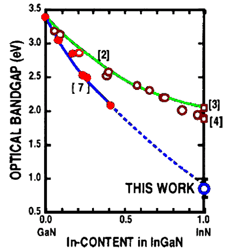
In1-xGaxN alloys. Photoluminescence
peak energy and band gap determined by optical absorption vs composition.
Some previously reported data on the Ga-rich side are also shown (Refs.6
and 7). All data are taken at room temperature unless otherwise noted.
The solid curve shows the fit to the band gap energies (abs and PT) by the equation Eg(x)=3.42x+ 0.77(1-x) - bx(1-x) with a bowing parameter b=1.43 eV. The dashed curve is the fit to the band gap energies on the Ga-rich side assuming a band gap of 1.9 eV for InN. Inset: Photoluminescencepeak energy plotted against absorption edge energy. The solid line is a least-square fit to experimental data on the Ga-rich side adopted from Ref. 8. The dashed straight line shows the relation when the Stokes shift is zero. Ref.6 - Pereira S. et al., Appl. Phys. Lett. 78, (2001) 2137; Ref.7 - Shan W. et al. J. Appl. Phys. 84, (1998) 4452; Ref.8 - O'Donnell K.P. et al., Phys. Status Solidi B 216, (1999) 141. Wu J., Walukiewicz W. et al. Appl. Phys. Lett. 80 (2002b) 4741 |
|
InxGa1-xN alloys. The relation between In content
and the band-gap energy. [2] - Osamura, K., Naka, S., and Murakami, Y., J. Appl. Phys. 46, (1975), 3432. [3] - Puychevrier N. & Menoret M., Thin Solid Films 36, (1976), 141. [4] - Tansley T. L. & Foley C. P., J. Appl. Phys. 59, (1986), 3241. [7] - Matsuoka T., Tanaka H., Sasaki T. & Katsui A., Proc. of the Sixteenth International Symposium on GaAs and Related Compounds, Karuizawa, Japan, 25-29 September 1989, Institute of Physics, Bristol (1990), p.141. Matsuoka et al. Appl. Phys. Lett. 81, (2002) 1246 Contact authors: T. Matsuoka |

|
InN, Wurtzite (hexagonal). Room-temperature absorption edge vs electron
concentration. The solid line is the calculated band gap assuming a nonparabolic (EP=10 eV) dispersion for the conduction band and including the band-renormalization effects. The dotted-dashed line is the same calculation but without including the band-renormalization effects. The dotted line is the result of a calculation assuming a parabolic (m*=0.07mo) conduction band. Inset: absorption (squared) curves for four samples with different free-electron concentrations (in cm-3). Wu J., Walukiewicz W., Shan W. et al. Phys. Rev. B 66 (2002c), 201403 Contact authors: W. Walukiewicz |

|
InN, Wurtzite (hexagonal). |
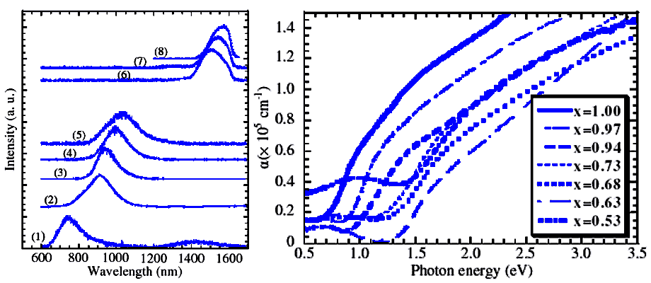 |
InxGa1-xN alloys. (a) Photoluminescence
spectra of films vs. In concentrations x. T=77 K. (1) - x = 0.37-0.47; (2) - x = 0.53; (3) - x = 0.63; (4) - x = 0.68; (5) - x = 0.73; (6) - x = 0.94; (7) - x = 0.97; (8) - x = 1.00. (b) Absorption spectra of InxGa1-xN films vs. photon energy. The temperature T=300 K (high indium composition region). Hori et al. Phys. Stat. Sol. (b) 234 (2002) 750 Contact authors: M. Hori & Y. Nanishi |
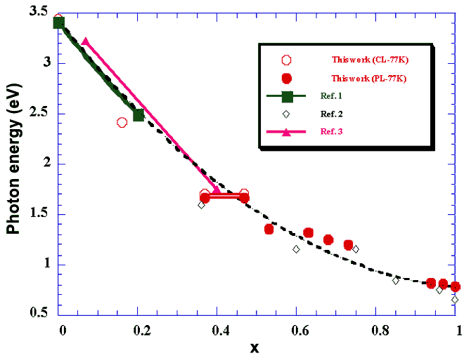 |
InxGa1-xN alloys. Luminescence peak positions
of catodoluminescence and photoluminescence spectra vs. concentration
x. The plots of luminescence peak positions can be fitted to the curve Eg(x)=3.48 - 2.70x - bx(1-x) with a bowing parameter of b=2.3 eV Ref.1 - Wetzel., Appl. Phys. Lett. 73, 73 (1998). Ref.2 - V. Yu. Davydov., Phys. Stat. Sol. (b) 230, R4 (2002). Ref.3 - O’Donnel., J. Phys .Condens. Matt. 13, 1994 (1998). Hori et al. Phys. Stat. Sol. (b) 234 (2002) 750 |
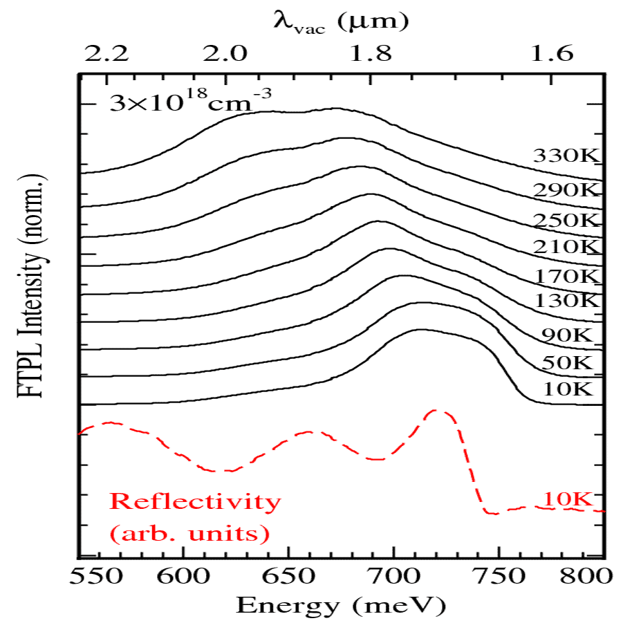 |
InN. PL spectra. The temperature dependence of the resonance
at the position of the Fermi edge for an InN layer doped with n=8x1017cm-3.
Basically two contributions can be seen in PL: One at the position of the renormalized gap (weak shoulder at ~650meV) and one at the position of the Fermi edge (~730meV) which is interpreted as a Mahan exciton. Feneberg et al., Phys. Rev. B 77 (2008), 245207 Contact authors: Klaus Thonke & Martin Feneberg |
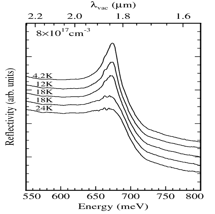 |
InN. A series of reflectance spectra recorded at different temperatures
is shown for a sample with n=3x1018cm-3. Feneberg et al., Phys. Rev. B 77 (2008), 245207 Contact authors: Klaus Thonke & Martin Feneberg These measurements confirm the low bandgap values of ~ 0.7 eV for InN at low temperature. |
| Remarks | Referens | ||
| Atomic distance of In-N dIn-N |
2.15 A | In K-edge EXAFS oscillation, film grown on sapphire using MBE |
Miyajima T. et al. (2002) |
| Atomic distance of In-In dIn-In |
3.53 A | In K-edge EXAFS oscillation, film grown on sapphire using MBE a-axis lattice constant a = 3.536 A (X-ray diffraction) c-axis lattice constant c = 5.701 A |
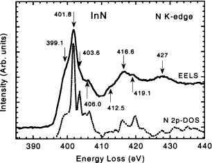 |
InN, Wurtzite (hexagonal). Solid line: Nitrogen K-edge from EELS measurements Dashed line: calculated nitrogen N 2p partial DOS. To eliminate small energy drift in STEM the spectrum is aligned with corresponding x-ray absorption data (Lawniczak-Jablonska K. et al., Appl. Phys. Lett. 70 (1997) 2711). The DOS calculations are aligned to EELS by displacing the primary peak to 401.8 eV for better comparison of the remaining features. The measured spectrum of the nitrogen K edge is in excellent agreement with calculated N 2p partial DOS of conduction band on the relative positions of major peaks. Mkhoyan et al. Appl. Phys. Lett. 82 (2003) 1407 Contact authors: K. Andre Mkhoyan |
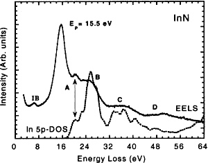 |
InN, Wurtzite (hexagonal). Single scattering distribution obtained
from low-loss EELS. The dashed line is calculated In 5p partial DOS of the conduction band convoluted with In 4d valence states. Measurements coupled with calculations indicate that these highly localized In 4d deep valence band states in wurtzite InN are 16.3±0.5 eV below the minimum of the conduction band. If we adopt the measured value of band gap of about 0.8 eV then the In 4d deep valence band states should be 15.5±0.5 below the top of the valence. From low-loss EELS, the position of the bulk plasmon-loss peak at 15.5 eV and strong interband transitions with energy 6.2 eV are also obtained. Mkhoyan et al. Appl. Phys. Lett. 82 (2003) 1407 |
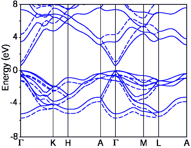 |
InN, Wurtzite (hexagonal). Energy band structure Solid lines: Density Functional Theory in Local Density Approximation (DFT-LDA) Dashed lines: including quasiparticlecorrections. Bechstedt et al. Phys. Stat. Sol. (a) 195 (2002) 628 |
|
|