![[English]](images/buttonr.gif)
| Russian | ||
|
English | |
|
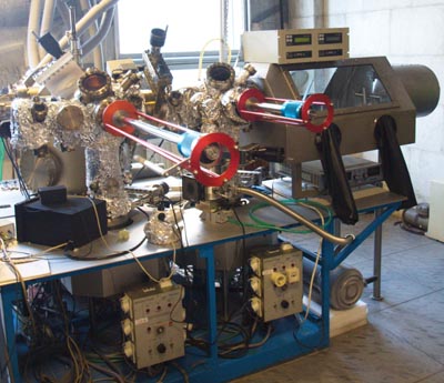
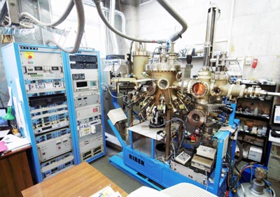
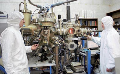
The MBE setup RIBER-32P ((Riber, France)
for growth of III-V semiconductor heterostructures (AlGaAsSb, InGaAsSb, InAsSb etc).
Growth chamber contains 8 molecular beam cells, including As valved cracking cell. The growth chamber has a
horizontal geometryand equipped with a quadrupole mass spectrometer for analysis of residual atmosphere.
The MBE setup is also equipped with modern diagnostic tools for growth control: reflection high energy electron
diffraction and IR pyrometer. The maximum available wafer diameter is 3 inches.
The setup has been fully re-equipped in 2002. Chemical cleaning of the cryopanel of the setup was performed in 2012. |
|
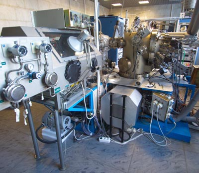
| The MBE setup SemiTEq STE3526 (supplied by "Semiconductor Technologies and Equipment" JSC, St.-Petersburg, Russia) for growth of wide gap II-VI heterostructures (ZnMgSSe, ZnCdSe, ZnCdTe, CdMgSe), as well as diluted magnetic semiconductors (II-Mn-VI). SemiTEq STE3526 MBE setup consists of two Growth Chambers (III-V and II-VI) with specific material sources, Load-Lock Chamber, Preparation Chamber with the possibility of preliminary annealing of substrates, and Storage buffer Chamber. The Growth Chambers are realized in a progressive vertical geometry commonly used by the major MBE equipment manufacturers. The maximum available wafer diameter is 2″, the epitaxy on ¼ of 2″ substrates also is possible. Veeco valved cracking cells are used as the Se and As sources. |
|
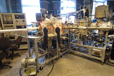
| The MBE setup Compact 21T ((Riber, France) (release 2004) for growth of III-Nitride heterostructures (AlGaInN doped with Si and Mg) with the improved accuracy of maintenance of technological parameters and unique opportunities of simultaneous use of plasma and high-temperature (ammonia cracking) techniques for nitrogen activation. 11 molecular beam sources are available. The setup is equipped with the following diagnostic-monitoring systems for growth: reflection high energy electron diffraction (RHEED), optical reflectometry, IR-pyrometry and optical emission spectrometry for recording of N2 plasma emission. The maximum available wafer diameter is 3 inches. |
|
Optimisation of InGaN epilayers grown by PA-MBE in COMPACT21
New growth method for InGaN based QW by PA-MBE in Compact 21