III-nitride structures and devices with quantum wells and superlattices
|
Since eighties the Group has been extensively studying optical and electronic properties of one- and two-dimensional defects, such as dislocations, grain boundaries and oxygen-induced stacking faults in Si, Ge, ZnSe and GaN. Recent years the Group concentrates on III-nitride physics and devices with quantum wells and superlattices. These materials and structures are enormous fundamental interest with great potential for optoelectronics.
The primary focusof our Research group work is on physics of extended defects in III-N nanostructures. Our current research interest in study of extended defects in GaN is greatly stimulated by rapid progress in the development of III-nitride optoelectronics.
The research activity of the Group includes:
Another direction of our group efforts is structural defects formed on surface of solids under mechanical stress. The fundamental mechanisms of destruction of elastically stressed materials at thermal and chemical activation of their surface are investigated. The kinetic mechanism of surface instability evolution during etching, corrosion, and growth is investigated. The role of stacking faults, dislocations and artificially created of surface steps in corrosion development of stressed Si crystals is studied. Photoluminescence of extended structural defects in semiconductorsOne of the semiconductor material science problems is the nature of electronic states, which are introduced by dislocations, or stacking faults. Recently we have suggested a deformation potential model to analyze electronic and optical properties of the extended defects. According to this model, the one-dimensional energy bands split off from the edges of the bulk bands by the strain field of the defects. Accordingly, the energy position of the dislocation-related photoluminescence is determined by the edge component of the dislocation Burgers vector.
The principal results which have been obtained using this approach are:
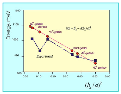
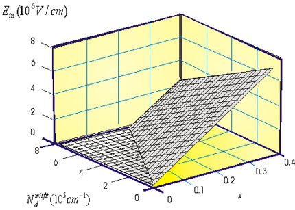
Misfit dislocations and radiative efficiency of InxGa1-xN/GaN quantum wellsThe most common defects in wurtzite GaN epilayers grown on sapphire are threading dislocations originated from high-lattice-mismatch between the epilayer and substrate. These defects can significantly affect the nonequilibrium carrier lifetime at low injection levels and prevent low laser thresholds. Recently, dislocations of another type, localized in the InxGa1-xN quantum wells, have been observed, which most probably are the misfit dislocations at GaN/InxGa1-xN interface. We investigate the influence of the misfit dislocations at the interface of the InxGa1-xN quantum well on the radiative efficiency of the carriers in quantum well.
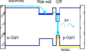
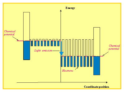
Charge Asymmetric Resonance Tunneling (CART) as a basic element of GaN based light-emitting diodeWe suggest a system of two wells with Charge Asymmetric Resonance Tunnelling (CART) as a basic element of light-emitting diode (LED) structure for semiconductors with different masses of electrons and holes.
The barrier design uses the charge asymmetric resonance-tunnelling phenomenon, which allows to make the barrier transparent for electrons and blocking for heavy holes. The phenomenon of the charge asymmetric resonance tunnelling uses the quantum mechanical effect of strong exponential dependence of the potential barrier tunnel penetrability on the mass of the tunnelling particle. First results of experimental investigation and theoretical modeling of the CART LED are obtained.
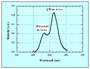
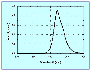
EL spectra at 20 mA from non-optimised (left) and optimised (right) CART structures. In the non-optimised structure, wide-well recombination occurs. In the optimised structure, only QW-related emission is observed. III-nitride Unipolar Light Emitting DevicesUnipolar light emitting device based on III-nitride superlattices for the generation of visible light is suggested. The main idea of the unipolar light emitting device (U-LED) is to create the analogue of an n-p junction between two n-type superlattices with a shallow and a deep subband.
This allows one to get electron transitions between two superlattices based on these alloys with energies in the range of 0 to 3 eV, which covers the visible and the infrared range of the spectra.
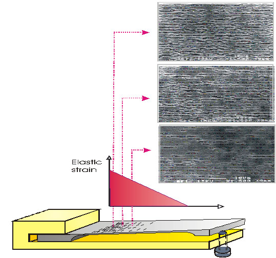
Physics of surface of elastically stressed solidsCorrosion precursors in the form of microgrooves appearing on the elastically compressed surface of a silicon plate under etching are observed and investigated. No corrosion precursors are observed on the elastically stretched surface. This distinguishes the observed effect from corrosion cracking of metals, during which corrosion usually takes place on stretched surfaces. The general dynamic model proposed for the evolution of surface microgrooves during etching, corrosion, and growth of elastically stressed solids is based on the concept of two local etching (growth) rates which are linear functions of the local stress tensor. The model describes the kinetics of the process, and the asymmetry of corrosion evolution to the deformation sign. The role of stacking faults, dislocations, and artificially created surface steps in the evolution of corrosion in stressed silicon crystals is studied.
For the first time the influence of magnitude and sign of elastic strain in a structures of crystal evaporated metal film on form and sizes of forming metal droplets and distances between droplets is found. The dependence of droplet sizes and distances between droplets on degree of deformation is observed at the stretched surface in the structure Si - In.
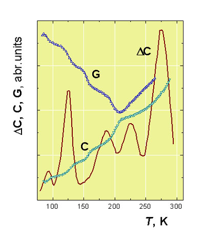
Despite many years of research, the nature of Si/SiO2 interface states remains controversial. It is known that oxygen- and hydrogen-induced defects have dramatic and complex effects in the Si-SiO2 system. It is clear that they also can play important role in nanostructures due to gettering at interfaces and dislocations. We studied surface conductivity in crystals of Ge and Si with structural defects using Schottky diodes with surface leakage channels. A set of sharp peaks and steps in the temperature curves of HF conductance and capacitance was observed. It was shown that all of the features are due to low-temperature changes of surface conductivity and reflect a set of interface states. These features were observed in Ge and Si at similar temperatures. The results compared with known data on behavior of hydrogen and oxygen in nanopores and at the surface of solids. It is concluded that intrinsic properties of oxygen- and hydrogen-containing complexes to rearrange the structure at low temperatures with change of the charge are responsible for observed features. We believe that the tendency to donor action of oxygen complexes due to increase of molecular bonds and hole self-trapping at low temperatures is the cause of low-temperature doping of near-surface layer of crystals.
References
Contact InformationContact Person: Professor Yuri Shreter
Phone: +7 (812) 247 9152, +7 (812) 247 3256
|