|
Silicon
Carbide Research Group
(
Headed by
Alexander
A. Lebedev,
Dr. of Sci.)
Main
goal
of the
group is to develop and investigate SiC-based
electronic devices.
|
|
Silicon Carbide
is a very perspective material for high
temperature, high frequency
and high power semiconductor
electronic devices. Large band gap, high thermal
conductivity,
high saturated electron drift velocity, very high breakdown
field, high
radiation hardness, and presence of intrinsic
oxide are the factors which have given
this material
its great potential in electronic device field.
In Silicon
Carbide Research Group,
technological base for industrial production
of high temperature SiC devices is created now.
|
|
STAFF
Principal
Researcher
Alexander
A. Lebedev,
Dr. of Sci.
|
Shura.lebe@mail.ioffe.ru
|
|
Leading
Researcher
Sergei
Yu. Davydov, Dr. of Sci.
|
sergei_davydov@mail.ru
|
|
Leading
Egineer
Alexandr A.
Lavrentev
Sergei
V Belov
Irina S.
Kotousova
|
AlLavren@yandex.ru
; Belov.Sergey@mail.ioffe.ru
koti@
pop.ioffe.rssi.ru
|
|
Senior
Researchers
Anatoly
M. Strelchuk, Candidate of Sci. (Ph. D.)
Marina G. Mynbaeva,
Candidate of Sci. (Ph. D.)
Eugenia V Kalinina,
Candidate of Sci. (Ph. D.)
Andrey S.
Zubrilov, Candidate of Sci. (Ph. D.)
|
Anatoly.strelchuk@pop.ioffe.rssi.ru
mgm@mail.ioffe.ru
evk.lebe@mail.ioffe.ru
asz.mail@mail.ru
|
|
Researchers
Elena V. Bogdanova
Natalia Yu.
Smirnova
Natalia V.Seredova
|
le.bog@mail.ioffe.ru
nata.s@mail.ioffe.ru
natasha.seredova@mail.ru
|
|
Junior
Researchers
Pavel
L. Abramov
Anton V. Sadokhin
|
pinski@list.ru
aln9t7o9n@mail.ioffe.ru
|
|
|
|
|
PhD
Students
Sergey
P. Lebedev
|
iegreg@mail.ru
|
|
MAIN
RESULTS
 Technology of SiC epilayers growth with given
parameters has been developed.
Technology of SiC epilayers growth with given
parameters has been developed.
Multi-layer n-p-n and n-p-n-p
structures have been obtained.
The processes of metalization were developed which allowed to
obtain the low
resistant ohmic contacts and Schottky diodes
with nearly "ideal" current-voltage characteristics.
The techniques of plasmo-ion etching of SiC
were developed .
Technology of device packaging was developed.
The concentration and main parameters of
native, artificially introduced, and
radiation defects were
investigated. The effect of these traps on recombination
processes in SiC epilayers and devices was studied.
Lifetimes and diffusion lengths of minority
carriers were investigated in SiC in
wide temperature range
from 77 K to 800 K.
Photoelectric characteristics of SiC p-n
structures and Schottky diodes were
investigated.
SiC-based
semiconductor devices of
many types were produced in
Silicon Carbide Research Group:
Schottky diodes, rectifier diodes, photodetectors, suppresser
diodes,
Field Effect Transistors (JFETs and MESFETs),
dynistors, nuclear detectors, IMPATT-diodes.
|
|
Main
technological process: Silicon Carbide Sublimation Epitaxy
SiC
epitaxial growth is carried out at pressure
10-6 Torr
in vertical quartz reactor
at temperature of 2000°
C.
|
|
ADVANTAGES
Sublimation etching
" in
situ "
at high temperature 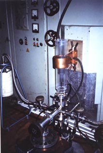
allows
to eliminate mechanical polishing of the surface. The height of
macro-steps on etched surface corresponds to a single 6H-SiC
cell (does not exceed 15-20A
).
Sublimation epitaxy can be used to reduce the
density
of structural defects in SiC substrates prepared by
modified Lely (ML) method. Epilayers grown on ML substrates with
uniformly distributed basal dislocations have higher structure
perfection than the native substrates (dislocation
density is decreased,
shallow pores are
closed).
Low-doped n-SiC epilayers
with
(Nd-Na)
~ (7-9)
x1014 cm-3
and hole diffusion
length of about 2.5-3
m m were
obtained.
High
growth rate of epitaxy of
about 20 m
m/h
was
achieved. Diodes with breakdown voltages up
to several
kilovolts and bipolar transistors with large coefficient gain
can be fabricated on the base of these epilayers.
Heteroepitaxial
growth of
epitaxial layers of 3C-SiC with operation area of
about ~
1cm2
and very high level of structural perfection
is possible on base
of 6H SiC substrates.
This technology can be successfully used for
growth thick high quality
epilayers on porous
SiC buffer.
Sublimation epitaxy setup can be used for
obtained nano-carbon films on SiC surface.
|
|
Recent
publications
(2005
-
2009)
|
|
This
page was last updated on
23-07-09.
Back
|