|
|
Staff of Group
|
e-mail
|
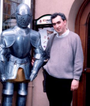
Andrei F.Tsatsulnikov
was born in St. Petersburg (at that time Leningrad), Russia in 1966
Education
- 1983-1989 - Leningrad Electrical Engineering Institute, A.F.Ioffe Physico-Technical Institute (Education Department)
- 1989-1992 - Post graduated course in Leningrad Electrical Engineering Institute, A.F.Ioffe Physico-Technical Institute (Education Department). Was awarded with Ph.D. degree in Physics and Math in 1992 - the title of Ph.D. thesis was „Structure and properties of deep acceptor centers, created by elements of copper subgroup in GaAs."
Career and research experience
- 1992 - present time - A.F.Ioffe Physico-Technical Institute, Research scientist.
Top
|
|
|
List of papers
e-mail
|
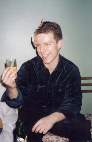
Wsevolod V. Lundin
was born in St. Petersburg (at that time Leningrad), Russia in 1972
Education
- 1979-1986 - State secondary school of St. Petersburg (at that time Leningrad)
- 1986-1988 - Physico-Technical school (a department of Ioffe Physico-Technical Institute)
- 1988-1995 - St. Petersburg Electrical Engineering University, department of Optoelectronics. My average mark was 5.0 at 5-degree scale. The title of my engineering diploma work was „Buried-heterostructure mesastripe lasers fabricated by meltback and regrowth in the same LPE process."
- 1995-1998 - Ph.D. study in St. Petersburg Electrical Engineering University, at the Optoelectronics department. Ioffe Physico-Technical Institute awarded me Ph.D. degree in Physics in October 1998. The title of my Ph.D. thesis was „Growth and characterization of GaN epitaxial layers and GaN/AlGaN heterostructures."
Career and research experience
- 1986-1989 - Intern in Ioffe Physico-Technical Institute at the position of junior laboratory assistant (out of staff). During that time, I got my first experience in research work.
- 1991-1995 - Intern in Semiconductor Quantum Electronics Laboratory, Ioffe Physico-Technical Institute, at the position of junior technologist (out of staff). During this work I got experience in LPE of AlGaAs and developed technology of fabrication of BH lasers with threshold current below 4 mA (with uncoated facets).
- 1995-1998 - Senior technologist at Scientific-Technological Center for Microelectronics at Ioffe Physico-Technical Institute. The subject of my study was development of MOCVD technology of GaN and related compounds.
- 1998-1999 - permanent staff position in Semiconductor Quantum Electronics Laboratory (headed by Prof. S.A.Gurevich), Ioffe Physico-Technical Institute. Subject of my responsibility was MOCVD growth of III-N structures as well as keeping MOCVD system in operating conditions.
- At present - permanent staff position in Physics of Semiconductor Heterostructures Laboratory (headed by academician Zh.I.Alferov), Ioffe Physico-Technical Institute. Subject of my responsibility is MOCVD process development of III-N structures.
May-July 1999 - visiting scientist in Technical University of Berlin
Area of expertise:
MOCVD growth of III-N semiconductors
Top
|
|
|
e-mail
|
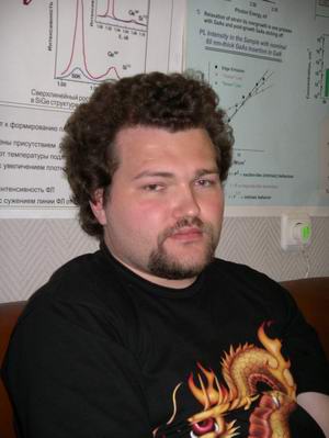
Alexei V. Sakharov
was born in St. Petersburg (at that time Leningrad), Russia in 1974
Education
- 1990 - graduated from Physico-Technical school (base school of the Ioffe Institute)
- 1996 - graduated with honors from the Physico-Technical Faculty (Department of Solid State Electronics) of St.-Petersburg State Technical University
- 2000 - Was awarded with Ph.D. degree in Physics and Math - the title of Ph.D. thesis was „Optical properties of GaN-based layers and heterostructures"
Career and research experience
- 1994 - present time - has been working in the area of III-V semiconductor heterostructures
- 1996 - present time - staff member of the Physico-Technical Institute
1998-2004 - visiting scientist in Technical University of Berlin, Germany (2 times) and Industrial Technology Research Institute, Hsinchu, Taiwan, R.O.C. (3 times)
Awards
- Soros Student Grant (1995-1996)
- Prize of the Science Council of the Ioffe Institute for work "InGaN/GaN/AlGaN Multilayer Structures and Surface-Emitting Devices Based on this Structures" (1999).
- Grant of President of Russia for support leading science schools and young scientists (2003-2004)
Top
|
|
|
List of papers
e-mail
|
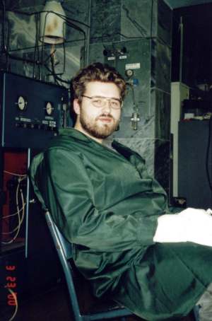
Evgeny E. Zavarin
Born: October 30, 1975
Martial Status: Married
Education
- 1982 - 1992 - State secondary school of St. Petersburg (at that time Leningrad)
- 1992 - 1996 – Bachelorhood, St. Petersburg State Electrotechnical University, department of Optoelectronics (supervised by Ioffe Physico-Technical Institute). The title of my bachelor work was „Growth of GaN epilayers by chloride epitaxy.“
- 1996 - 1998 Magistracy, St. Petersburg State Electrotechnical University, department of Optoelectronics. The title of my master work was.”Growth of GaN epilayers on amorphous substrates by chloride epitaxy.” After Magistracy, my degree is Master of science and technology.
- 1998 - 2001 - Ph.D. student in St. Petersburg State Electrotechnical University, at the Optoelectronics department. The subject of my study is development of MOCVD technology of GaN and related compounds.
Career and research experience
- 1995 - 1999 - junior researcher in Physics Phenomena in Semiconductor Heterostructures Laboratory (headed by Prof. Yu.V.Zhilyaev), Ioffe Physico-Technical Institute. Subject of my responsibility was growth of GaN epilayers by chloride epitaxy.
- 1999 - 2001 - Ph.D. student in Physics of Semiconductor Heterostructures Laboratory (headed by academician Zh.I.Alferov), Ioffe Physico-Technical Institute. Subject of my responsibility is MOCVD process development of III-N structures.
- At present - Scientist in Physics of Semiconductor Heterostructures Laboratory (headed by academician Zh.I.Alferov), Ioffe Physico-Technical Institute. Subject of my responsibility is MOCVD process development of III-N structures.
The main results of my activity are as follow:
– Growth free standing GaN epilayers by chloride epitaxy on various substrates.( 1996-1999)
– Study of growth peculiarities of GaN epilayers by MOCVD technique on free standing GaN layers. (1999-2000)
– Devolopment of in-situ optical reflectance monitoring system for MOCVD growth (1999-2000).
– InGaN/GaN/AlGaN MQW LED’s (415-465 nm) with effectiveness ~ 2-3% (on-wafer probing) (2000).
– Superlattices AlGaN/GaN, AlN/GaN, AlGaN/AlN with various periods (2002)
– Heterostructures AlGaN/GaN, AlN/GaN (2003)
– Study of growth peculiarities of GaN epilayers on various nucleation layers. (2003)
Top
|
|
|
List of papers
e-mail
|
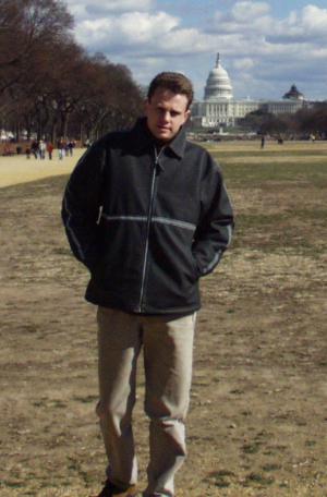
Alexander V. Fomin
Education
- 1995 MS in Chemistry, St-Petersburg State University, Russia
Career and research experience
- 1994-1995 Department of Chemistry St-Petersburg State University
Laboratory Assistant
- - fundamental research on colloid chemistry and surface science.
- 1997-1999 ECROS, Ltd.
Engineer-Chemist
- - engineering of pure inorganic compounds processes
- - qualitative and quantitative analysis of inorganic compounds
- 1999-2001 Ioffe Physico-Technical Institute, Russian Academy of Sciences,Semiconductor devices laboratory
Researcher
- - Hydride Vapor Phase Epitaxy (HVPE) of III-N compound semiconductorsOperated on HVPE experimental reactor. Deposition and characterization of GaN, AlGaN, AlN epilayers. Research on n and p-type doping during HVPE process
- 2001-2002 Technologies and Devices International, Inc.(MD, USA)
Chemist
- - Hydride Vapor Phase Epitaxy of III-N compound semiconductors Research on homoepitaxial deposition by HVPE on freestanding GaN
- - development of the pretreatment procedure for GaN substrates.
- 2002-present Ioffe Physico-Technical Institute, Russian Academy of Sciences,Physics of Semiconductor Heterostructures laboratory
MOCVD group Engineer
- - MOCVD technology of III-N compounds
Top
|
|
|
e-mail
|
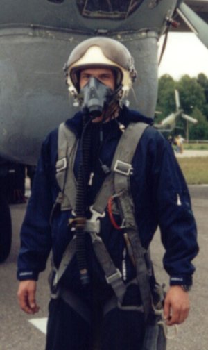
Dennis A. Bedarev
was born in Maikop, Russian Federation in 1972
Education
- 1986-1992 - Electromechanical technical school of Leningrad (specialization: electrical equipment of industrial enterprises)
- 1993-1998 - Nord-West Correspondence Polytechnical Institute, evening school (specialization: industrial electronics) with honors.
Career and research experience
- 1992-1998 - electrician, Electromechanical factory
- 1996-1998 - Junior laboratory assistant (out of staff) at Ioffe Physico-Technical Institute
- 1998-2000 - Laboratory assistant, permanent staff position in Ioffe Physical-Technical Institute
- 2000-present time - Junior Research Scientist in Ioffe Physical-Technical Institute
Interests
- Designing, making and modernization of scientific and technological eguipment
- Optical characterization of III-V and III-N heterostructures
- Postgrowth processing methods of semiconductors devices
Top
|
|
|
