|
|
Processing Equipment
Facilities for the rapid processing of the III-N structures are in the stage of development.
Etching system
Era-5M TCP system for chemical ion etching.
manufacturer: ESTO-Vacuum. Russia.
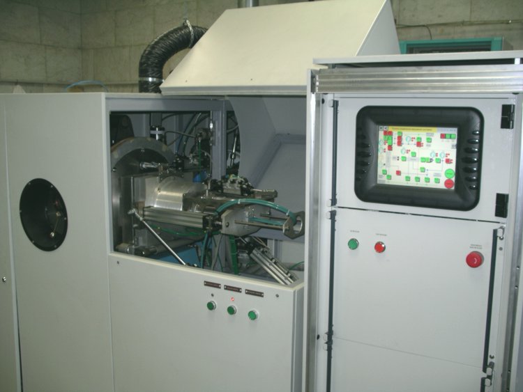
Technical data:
- Capacity: up to 6x2-inch substrates
- Samples position: vertical
- Charging by way of lock-chamber
- Turbo-molecular pump (low pressure 5x10⁻⁵ Pa)
- Separate whater heating and cooling for holder and camera.
- In-situ optical reflectance monitoring in the near-normal incident using Laser LED and Si photodetector.
- The etching process are operated by manually or fully automatic system.
Etching conditions:
- RF power: 100...800 W
- Ion energy: 0,8...400 eV
- Working pressure: 1...1x10-2 Pa
- Gases: Ar, N2, O2, Cl2, BCl3, SF6 and 2 reserve channels.
|
|
Contact evaporation system
under modernization
|
|
System of thinning of samples
the stage of construction.
|
|
Laboratory cutting system
the stage of development.
|
|
|
Lithography facilities available in the cooperation with other Labs.
|
|
|
Processing of device structures is carried out with cooperation of Laboratory of Semiconductor Quantum Electronics
|
|
|